In the vast realm of circuit design, navigating the intricate pathways and intricacies can often feel like embarking on an uncharted journey. However, with the aid of advanced PCB layout and simulation tools, these treacherous terrains can be conquered with precision and finesse.
This article delves into the art of mastering circuit design by exploring how these tools elevate designs to new heights. By harnessing their power, engineers can not only streamline efficiency but also maximize design quality, ultimately unlocking the full potential of their creations.
Key Takeaways
- Schematic capture software empowers engineers to manipulate and refine their designs before physical implementation, allowing for exploration and experimentation.
- Signal integrity considerations such as impedance matching, crosstalk interference, grounding, and shielding are crucial for maintaining signal integrity and minimizing noise.
- Power and ground planes play a vital role in minimizing noise, providing stable power distribution, and reducing EMI.
- Simulation tools save time by eliminating the need for physical prototyping, enabling design optimization, and resulting in higher quality products with faster time-to-market.
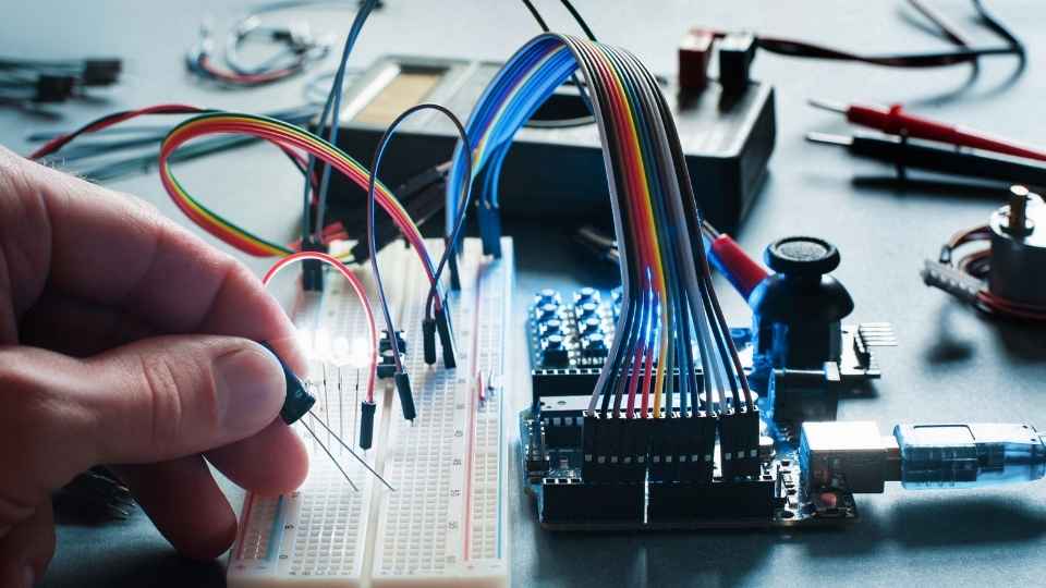
The Power of Schematic Capture
The use of schematic capture software allows engineers to efficiently translate their circuit design ideas into a visual representation, facilitating the development and optimization of complex electronic systems. This powerful tool enables engineers to create a detailed blueprint of their circuit designs, capturing all the necessary components, connections, and specifications.
By utilizing schematic capture software, engineers can easily manipulate and refine their designs, making adjustments as needed before moving on to the physical implementation stage. This level of precision and control greatly enhances the efficiency and accuracy of the design process.
Schematic capture software also offers freedom in terms of exploration and experimentation. Engineers can quickly test different configurations and variations of their circuits without having to physically build each prototype. This flexibility allows for faster iteration cycles and promotes innovation by enabling designers to explore multiple design possibilities within a short timeframe.
Overall, the use of schematic capture software empowers engineers with greater control over their circuit design process while providing them with the freedom to explore new ideas and optimize their designs efficiently.
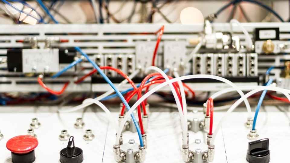
Navigating the Nuances of PCB Layout
Navigating the nuances of PCB layout requires careful consideration and attention to detail. Component placement techniques play a crucial role in optimizing signal integrity and minimizing noise interference.

Additionally, power and ground planes must be strategically implemented to ensure proper distribution of power and maintain a low impedance path for return currents.
Component Placement Techniques
Optimizing component placement is a critical aspect of circuit design that can greatly impact the overall performance and efficiency of the PCB layout. Proper placement of components can minimize signal interference, reduce noise coupling, and enhance thermal management. When considering component placement techniques, it is important to consider factors such as signal integrity, power distribution, and heat dissipation.
By strategically placing components based on their electrical characteristics and physical requirements, engineers can achieve optimal performance while minimizing board size and complexity.
One technique commonly used for component placement is called 'star grounding,' where all ground connections are brought to a central point to minimize ground loop effects. Another technique involves grouping components according to their function or signal flow to reduce trace length and improve signal integrity. Additionally, careful consideration should be given to high-power components that generate significant heat, ensuring they have adequate space for proper cooling.
Overall, optimizing component placement requires careful analysis of various factors and considerations during the design process. Utilizing advanced PCB layout and simulation tools can facilitate this optimization by providing accurate models, allowing engineers to visualize potential issues before fabrication begins. By mastering these techniques, designers can elevate their designs' performance and efficiency while maintaining the desired freedom in circuit design choices.
Signal Integrity Considerations
To ensure optimal signal integrity in circuit design, engineers must carefully analyze and address various factors that can affect the quality and reliability of signals. This involves considering the following:
Impedance matching: Matching the impedance of the source, transmission lines, and load is crucial for minimizing signal reflections and maximizing power transfer. Failure to achieve impedance matching can result in signal degradation or even complete signal loss.
Crosstalk: Crosstalk occurs when signals interfere with each other due to electromagnetic coupling between adjacent traces on a PCB. Proper spacing and routing techniques must be implemented to minimize crosstalk effects.
Grounding and shielding: Effective grounding and shielding are essential for reducing noise and maintaining signal integrity. Proper ground plane placement, isolation techniques, and use of shielded cables help mitigate interference from external sources.
Power and Ground Planes
Effective implementation of power and ground planes is crucial in circuit design for minimizing noise, providing stable power distribution, and maintaining signal integrity. Power planes are used to distribute power throughout the circuit while ground planes serve as a reference point for electric currents. By employing these planes effectively, designers can reduce electromagnetic interference (EMI) and ensure reliable operation of their circuits.
One key advantage of using power and ground planes is that they offer low impedance paths for high-frequency return currents. This helps prevent voltage drops and minimizes noise coupling between different components on the board. Additionally, placing power and ground planes adjacent to each other creates a controlled capacitance that further aids in noise reduction.
To harness the magic of simulation tools, engineers can use software programs like SPICE (Simulation Program with Integrated Circuit Emphasis). These tools allow designers to analyze various aspects of their circuits such as signal integrity, power distribution, EMI/EMC compliance, and thermal performance before fabrication. Simulation tools enable thorough testing and optimization of designs, saving time and resources during the development process.
Simulation tools provide engineers with the ability to test and validate their circuit designs, allowing for greater accuracy and efficiency in the development process. These powerful tools offer numerous benefits that can greatly enhance the design workflow:
Time Savings: Simulation eliminates the need for physical prototyping, saving valuable time in the design cycle.

Cost Reduction: By identifying potential issues early on, simulation tools help prevent costly mistakes and rework.
Design Optimization: Simulations enable engineers to fine-tune their designs and explore different configurations, leading to improved performance.
By leveraging simulation tools, engineers can confidently iterate and refine their circuit designs before committing them to production, resulting in higher quality products and faster time-to-market.
With a solid foundation in place through simulation, the next step is streamlining efficiency with BOM generation...
Streamlining Efficiency With BOM Generation
Streamlining efficiency with BOM (Bill of Materials) generation is a critical aspect of optimizing the product development process. By automating parts procurement, engineers can save valuable time and resources while ensuring accurate bill creation.
Additionally, leveraging BOM generation tools enables better supply chain management, allowing for improved collaboration and coordination with suppliers.
Automating Parts Procurement
To enhance efficiency in the circuit design process, automating parts procurement can significantly reduce the time and effort required to source and acquire necessary components. By leveraging automation tools, designers can streamline their workflow and focus on other critical aspects of the design process.
Here are three reasons why automating parts procurement is essential:
Time-saving: Automation eliminates manual searching and ordering, saving valuable time that can be allocated to design optimization or testing.
Cost-effective: Automated systems compare prices from multiple suppliers, ensuring competitive pricing for components without compromising quality.
Accuracy: Automation reduces human error by providing real-time availability and cross-referencing component specifications with current designs.
Enhancing Bill Accuracy
By ensuring precise and detailed bill accuracy, designers can effectively manage costs and avoid unnecessary delays in the circuit design process. A bill of materials (BOM) is a crucial document that lists all the components required for a circuit design. Any errors or omissions in the BOM can lead to costly rework or delays in procurement.
To enhance bill accuracy, designers can leverage advanced PCB layout and simulation tools. These tools provide features such as automated component placement, real-time part validation, and integration with manufacturer databases. With these capabilities, designers can ensure that all necessary components are included in the BOM and that they meet specified requirements.
Additionally, these tools enable designers to track component availability and pricing information, allowing them to make informed decisions about part selection and sourcing. By enhancing bill accuracy, designers gain greater control over their designs while minimizing costs and avoiding potential setbacks during fabrication.

Improving Supply Chain Management
Effective supply chain management is essential for ensuring timely delivery of components and minimizing production delays. In today's fast-paced business environment, companies must optimize their supply chains to stay competitive.
Here are three key benefits of improving supply chain management:
Enhanced Efficiency: By streamlining processes and reducing waste, companies can achieve higher levels of efficiency in their supply chains. This translates into cost savings, improved customer satisfaction, and increased profitability.
Improved Collaboration: A well-managed supply chain fosters collaboration between suppliers, manufacturers, and distributors. Effective communication and coordination lead to better decision-making, reduced lead times, and seamless integration across the entire value chain.
Increased Flexibility: A resilient supply chain allows companies to quickly adapt to changing market conditions or unexpected disruptions. By having multiple sourcing options and alternative distribution channels in place, organizations can mitigate risks and maintain uninterrupted operations.
Maximizing Design Quality Through Netlist Export
One method for maximizing design quality is through the strategic utilization of netlist export during the circuit design process.
Netlist export refers to the process of creating a list of all the electrical connections and components in a circuit design, which can then be used for further analysis and simulation.

By exporting the netlist, designers gain the freedom to explore various aspects of their circuit's performance, such as signal integrity, power distribution, and electromagnetic compatibility.
This allows them to identify potential issues and make necessary optimizations before moving on to PCB layout.
With accurate netlist export, designers can effectively leverage simulation tools to validate their designs against desired specifications, ensuring optimal performance and functionality.
Ultimately, this approach empowers designers with greater control over their circuits' quality and enhances overall design efficiency.
Tips and Tricks for Mastering PCB Layout and Simulation
Utilizing industry best practices, engineers can enhance their understanding and proficiency in optimizing the layout and performance of printed circuit boards. By following these tips and tricks, engineers can elevate their designs to new heights:
Plan Ahead: Taking the time to carefully plan the layout of a PCB can save significant time and effort in the long run. Consider factors such as component placement, signal integrity, and thermal management.
Use Design Tools: PCB layout and simulation tools offer engineers the freedom to experiment with different design options before committing to a final layout. These tools provide insights into potential issues early on, allowing for timely adjustments.

Collaborate with Peers: Engaging in discussions with other experienced engineers can lead to valuable insights and fresh perspectives. Sharing knowledge and experiences within a community fosters continuous learning and improvement.
By harnessing the capabilities of advanced software and resources, engineers can unlock new possibilities in circuit design and maximize the potential of their PCB projects. With the aid of powerful PCB layout and simulation tools, designers can streamline their workflow, improve accuracy, and enhance overall efficiency.
These tools provide a range of features that allow for precise placement and routing of components, efficient power distribution, signal integrity analysis, thermal management optimization, and much more. By utilizing these tools effectively, engineers can minimize design iterations, reduce time-to-market, and achieve higher quality designs.
The freedom offered by these tools allows engineers to explore innovative techniques such as 3D modeling and virtual testing to validate their designs before physical prototyping. Ultimately, leveraging PCB layout and simulation tools empowers engineers to push the boundaries of circuit design and create cutting-edge solutions with confidence.
Frequently Asked Questions
What Are Some Common Challenges Faced During PCB Layout and How Can They Be Overcome?
Common challenges faced during PCB layout include signal integrity issues, component placement constraints, and thermal management. These can be overcome by using advanced simulation tools, careful planning, optimized routing techniques, and close collaboration between design teams.
Schematic capture and PCB layout tools differ in their functions. Schematic capture focuses on creating the logical representation of a circuit, while PCB layout tools deal with translating that representation into a physical design for manufacturing.
Simulation tools are invaluable in identifying and resolving potential electrical issues in circuit designs. By allowing engineers to virtually test and analyze their designs, these tools aid in optimizing performance, reducing risks, and improving overall design efficiency.

What Factors Should Be Considered When Generating a Bill of Materials (Bom) for a PCB Design?
When generating a bill of materials (BOM) for a PCB design, factors such as component availability, cost, compatibility, and quality should be considered. Accurate BOM management is crucial to ensure successful and efficient circuit designs.
How Does Netlist Export Contribute to Ensuring Accurate and Efficient Circuit Design?
Netlist export contributes to accurate and efficient circuit design by generating a list of all the connections between components in a design. This allows designers to simulate, analyze, and troubleshoot circuits more effectively, ensuring proper functionality and minimizing errors.
 Basic Electronics ConceptsEssential ToolsCircuit Design BasicsMicrocontrollersDIY Electronics ProjectsRoboticsPrivacy PolicyTerms And Conditions