Are you ready to take your PCB design skills to the next level?
In this article, we will explore the secrets of hardware designers who have mastered the art of perfecting their designs using modern techniques.
From understanding the basics of PCB design to implementing cutting-edge layout strategies and optimizing signal integrity, we will delve into every aspect of creating flawless printed circuit boards.
Get ready to elevate your design game with this comprehensive guide tailored for aspiring hardware designers seeking freedom and excellence in their craft.
Key Takeaways
- Familiarity with industry-standard software tools such as CAD programs is necessary for PCB design.
- Implementing modern techniques such as HDI technology, microvias, blind/buried vias, and differential pair routing improves PCB performance.
- Optimizing signal integrity through impedance matching, solid ground planes, decoupling capacitors, and noise minimization is crucial.
- Proper component placement, trace routing, grounding techniques, and the use of advanced CAD tools are essential for optimal performance and reliability.
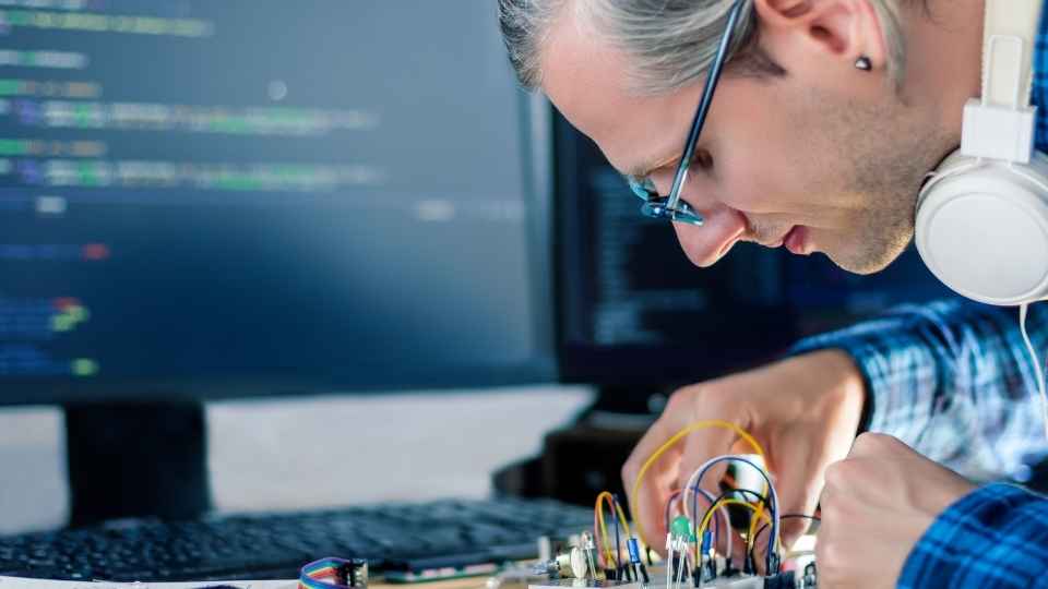
Understanding the Basics of PCB Design
To effectively optimize your PCB design using modern techniques, it is crucial to first gain a solid understanding of the basics of PCB design. This foundation will serve as a springboard for implementing advanced strategies and ensuring the success of your project.
At its core, PCB design involves creating a layout that connects electronic components through conductive pathways on a board. It requires knowledge of electrical engineering principles, circuit design considerations, and manufacturing constraints. Familiarity with industry-standard software tools such as CAD programs is also essential.
Understanding the fundamentals includes grasping concepts like component placement, trace routing, power distribution, and signal integrity. It involves selecting appropriate materials and considering environmental factors like temperature and humidity.
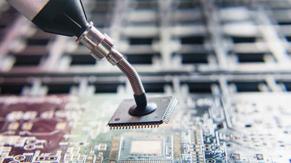
Implementing Modern Techniques for PCB Layout
Implementing cutting-edge methodologies in PCB layout enables the seamless integration of advanced features and ensures optimal performance of electronic circuits. Modern techniques have revolutionized the field of PCB design, providing hardware designers with tools to create highly efficient and reliable circuit boards.
One such technique is the use of high-density interconnect (HDI) technology, which allows for increased component density and reduced signal distortion. By utilizing microvias and blind/buried vias, designers can achieve smaller form factors without compromising functionality.
Another important technique is impedance control, which ensures that signals propagate correctly through transmission lines. By carefully calculating trace widths and layer stackup, designers can maintain consistent impedance values throughout the board.
Furthermore, employing differential pair routing techniques helps mitigate noise interference and improves signal integrity in high-speed communication interfaces like USB or Ethernet.
Optimizing Signal Integrity in PCB Designs
Signal integrity is a critical consideration in PCB designs as it ensures the accurate and reliable transmission of electronic signals. To optimize signal integrity, hardware designers can employ modern techniques that help minimize noise and distortion.
Here are three key strategies to achieve this:
Proper impedance matching: Ensuring that the impedance of the transmission lines matches the characteristic impedance of the PCB helps reduce reflections and signal degradation.

Grounding techniques: Implementing a solid ground plane, minimizing ground loops, and using separate analog and digital ground planes help prevent interference and crosstalk between different circuit components.
Decoupling capacitors: Placing decoupling capacitors strategically near sensitive components helps stabilize power supply voltages, reducing noise caused by voltage fluctuations.
Best Practices for Component Placement and Routing
An effective strategy for optimizing component placement and routing in PCB designs is to carefully consider the proximity and orientation of critical components to minimize signal interference. By placing high-speed components closer together, trace lengths can be minimized, reducing the potential for signal degradation and improving overall signal integrity. Additionally, it is important to pay attention to the orientation of sensitive analog or RF components, as their performance can be affected by nearby noise sources. Proper grounding techniques should also be implemented to minimize ground loops and ensure a clean return path for signals. Advanced CAD tools allow designers to visualize and analyze these aspects before finalizing the layout. Considering these best practices during the design phase can significantly improve the performance and reliability of PCBs.
Transitioning into the subsequent section about testing and validation of PCB designs, once the component placement and routing are optimized, it is crucial to thoroughly test and validate the design to ensure its functionality meets specifications.
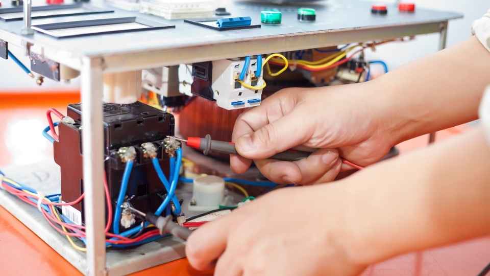
Testing and Validation of PCB Designs
Testing and validation of PCB designs are essential steps in the design process to ensure that the functionality and performance meet the required specifications. This stage involves thorough examination of the PCB layout, electrical connectivity, signal integrity, and overall system functionality.
To perfect your PCB design using modern techniques, consider the following:
Functional Testing:

Verify all components are correctly placed and soldered.
Check for proper power distribution and signal routing.
Test for expected output signals.
Performance Testing:
Analyze signal integrity through simulation tools.
Perform high-speed testing to verify data transmission quality.
Evaluate thermal performance under various load conditions.
Compliance Testing:
Ensure compliance with industry standards (e.g., EMC/EMI).
Validate safety requirements (e.g., insulation resistance).
Frequently Asked Questions
How Can I Choose the Right Components for My PCB Design?
To choose the right components for your PCB design, you should consider factors such as functionality, compatibility, reliability, cost-effectiveness, and availability. Conduct thorough research and analysis to ensure optimal performance and successful integration into the overall system.
What Are Some Common Mistakes to Avoid When Laying Out a Pcb?
When laying out a PCB, it is crucial to avoid common mistakes that can lead to issues such as signal interference or component placement errors. By following best practices and considering factors like trace routing and power distribution, designers can ensure a successful PCB layout.
Are There Any Specific Design Considerations for High-Speed PCB Designs?
When designing high-speed PCBs, it is crucial to consider signal integrity, impedance control, and noise reduction techniques. Proper routing and placement of components are essential for minimizing signal degradation and ensuring optimal performance.
How Can I Ensure Signal Integrity in My PCB Design?
To ensure signal integrity in a PCB design, it is crucial to consider factors such as impedance control, proper power distribution, minimizing noise and crosstalk, using ground planes and decoupling capacitors, and performing thorough testing and simulation analysis.
What Are the Best Practices for Thermal Management in PCB Designs?
Best practices for thermal management in PCB designs include proper component placement, heat sinks, thermal vias, and copper pours. Additionally, using multi-layer boards with internal power and ground planes can help distribute heat more effectively.
 Basic Electronics ConceptsEssential ToolsCircuit Design BasicsMicrocontrollersDIY Electronics ProjectsRoboticsPrivacy PolicyTerms And Conditions