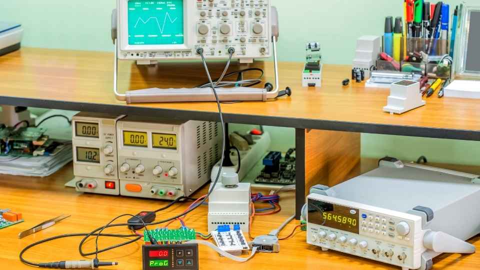
As an avid PCB enthusiast, I've always been fascinated by the intricate process of crafting perfect boards. From designing layouts to mastering soldering techniques, there's a world of precision and creativity waiting to be explored.
In this article, we'll delve into the art of PCB crafting and go beyond the basics. Join me as we uncover advanced tips and tricks for optimizing signal integrity, tackling surface mount components, and ultimately achieving flawless PCBs that bring our electronic creations to life.
Key Takeaways
- Meticulously place components, traces, and connections for optimal performance and reliability
- Follow specific rules and guidelines for layout design and optimization
- Consider factors like power distribution, heat dissipation, and impedance matching
- Utilize proper soldering techniques, including temperature control, flux application, and steady hands, for reliable and robust connections
Understanding PCB Layout Design
Understanding PCB layout design is essential for creating a well-functioning circuit board. As an engineer, I believe that the layout design plays a crucial role in determining the performance and reliability of the final product.
Every component, trace, and connection must be meticulously placed to ensure optimal signal integrity and minimize interference. The placement of components should follow specific rules and guidelines to achieve the desired functionality while considering factors like power distribution, heat dissipation, and electromagnetic compatibility.
Additionally, attention must be given to routing traces carefully and efficiently to avoid signal crosstalk or noise.
With a thorough understanding of PCB layout design principles, one can create circuits that not only meet technical requirements but also provide the freedom for future modifications or enhancements if needed.
Mastering Tracing Techniques for Perfect PCBs
When it comes to creating perfect PCBs, mastering tracing techniques is essential. The width of the traces must be carefully considered to ensure proper signal integrity and minimize impedance mismatches.

Trace Width Considerations
To ensure optimal performance in your PCB design, you'll need to pay attention to trace width considerations. The width of the traces on your printed circuit board plays a crucial role in determining its electrical characteristics and overall functionality.
Here are five key points to keep in mind:
Current carrying capacity: The trace width should be chosen based on the amount of current it needs to carry without overheating.
Voltage drop: A narrower trace can lead to higher resistance and voltage drops, affecting signal integrity and power delivery.
Signal integrity: Wider traces help reduce impedance and signal degradation, especially for high-speed signals.
Manufacturability: Consider the capabilities of your manufacturer when selecting trace widths to ensure they can be reliably produced.
Space constraints: Designing with limited space may require you to optimize trace widths for efficient use of available area.

Signal Integrity Optimization
Improving signal integrity is crucial for ensuring optimal performance in your PCB design. One way to achieve this is by carefully selecting wider trace widths.
By increasing the width of the traces on your PCB, you can reduce resistance and minimize voltage drops, resulting in improved signal transmission.
Wider traces also help to decrease crosstalk between neighboring signals, reducing the risk of interference and maintaining signal integrity.
It's important to consider factors such as current carrying capacity and impedance control when determining the appropriate trace width for your design.
Additionally, using wider trace widths allows for easier manufacturing and assembly processes, providing more freedom in selecting components and optimizing the overall layout of your PCB.
Overall, carefully choosing wider trace widths plays a significant role in optimizing signal integrity while offering flexibility in designing high-performance PCBs.
Minimizing Impedance Mismatches
Minimizing impedance mismatches is essential for maintaining signal integrity in PCB designs. One way to achieve this is by carefully selecting matching transmission line widths. This ensures that the electrical signals propagate smoothly without reflections or distortions.
Here are five key factors to consider when choosing transmission line widths:
Proper impedance calculation: Accurate calculation of the required characteristic impedance based on the dielectric constant and trace dimensions.
Controlled impedance manufacturing: Ensuring that the fabrication process maintains consistent trace width and spacing, often achieved through controlled etching or laminated substrates.
Crosstalk reduction: Designing appropriate spacing between adjacent traces to minimize electromagnetic interference (EMI) and crosstalk.
Trace length matching: Keeping trace lengths equal or within specified tolerances to prevent timing issues and signal skew.
Signal termination: Employing proper termination techniques at both ends of transmission lines to prevent signal reflection.
Exploring Through-Hole Soldering Methods
When it comes to exploring through-hole soldering methods, I find myself diving into a world of precision and intricacy.

Through-hole soldering techniques offer a reliable and sturdy connection between components and the PCB, ensuring long-lasting functionality.
Soldering Techniques for Through-Hole
There's no denying that mastering soldering techniques is essential for achieving quality through-hole connections on PCBs. Here are some key techniques to help you achieve flawless solder joints:
Properly preparing the components and PCB: Ensure both surfaces are clean and free from any contaminants before soldering.
Using the right soldering iron temperature: Different components require different temperatures, so it's important to find the optimal temperature for each joint.
Applying the right amount of solder: Too little or too much solder can result in weak connections or short circuits, respectively.
Maintaining a steady hand and good technique: A stable hand and precise movements are crucial for accurate placement and controlled application of solder.
Ensuring proper heat transfer: Heat must be evenly distributed between the component lead, pad, and solder to create a strong bond.

Mastering these techniques won't only improve your through-hole soldering skills but also enhance the overall quality and reliability of your PCBs.
Benefits of Through-Hole Soldering
Now let's dive into the benefits of through-hole soldering.
As an avid electronics enthusiast, I appreciate the sense of freedom this technique brings to my projects. Through-hole soldering provides robust and reliable connections, ensuring a sturdy bond between components and the PCB. This method allows for easy repairs and modifications, making it ideal for prototyping or troubleshooting circuits.
Additionally, through-hole components offer better heat dissipation due to their larger physical size, resulting in improved long-term reliability. Furthermore, this technique allows for greater accessibility and compatibility with a wide range of electronic devices.
With through-hole soldering, I can confidently assemble intricate circuitry while enjoying the flexibility to experiment and explore new possibilities in my electronic creations.
Troubleshooting Common Soldering Issues
If you're experiencing solder joints that look dull and lumpy, it's likely due to insufficient heat or improper soldering technique. To help troubleshoot common soldering issues, here are some tips to ensure your connections are flawless:
Ensure proper heat: Use a temperature-controlled soldering iron set to the correct temperature for your components.

Cleanliness is key: Make sure your components and PCB are clean before soldering, as dirt and debris can affect the quality of the joint.
Use flux: Apply flux to both the component lead and the pad on the PCB to improve wetting and enhance the flow of solder.
Avoid excessive heat exposure: Prolonged heat exposure can damage sensitive components, so keep your iron in contact with the joint for only as long as necessary.
Practice good technique: Use steady hands, apply even pressure, and make sure your iron tip is properly tinned.
Advanced Techniques for Soldering Surface Mount Components
Using advanced techniques, you'll need to master soldering surface mount components for perfect PCBs. These components are smaller in size and require precision during the soldering process.
Start by preparing your workspace with good lighting and a magnifying glass to ensure accuracy. Apply flux to the pads on the PCB to enhance solder flow and prevent bridges between adjacent pads. Use a fine-tipped soldering iron with temperature control to avoid overheating or damaging the components.
Place small amounts of solder onto the tip of the iron and touch it lightly against the pad, allowing it to flow onto both the pad and component lead simultaneously. Finally, inspect your work using a microscope or magnifying glass to identify any potential issues before moving on.

With practice, these advanced techniques will help you achieve flawless PCBs.
Optimizing PCB Layouts for Signal Integrity
To optimize PCB layouts for signal integrity, it's important to consider factors such as trace length, component placement, and ground plane design. These elements play a crucial role in ensuring reliable transmission of electronic signals on the printed circuit board. Here are five key considerations when designing PCB layouts for signal integrity:
Trace Length: Keeping traces as short as possible minimizes signal degradation and improves overall performance.
Component Placement: Properly positioning components reduces parasitic capacitance and inductance, enhancing signal integrity.
Ground Plane Design: A solid ground plane helps reduce noise and provides a reference point for all signals on the board.
Signal Routing: Carefully routing signals to avoid crosstalk and interference is vital for maintaining signal integrity.
Impedance Matching: Ensuring impedance matching between different components and traces prevents reflections and signal distortions.

Beyond the Basics: Advanced Tips and Tricks for Perfect PCB Crafting
Now that we've covered the basics of PCB crafting and optimizing layouts for signal integrity, let's dive into the exciting world of advanced tips and tricks.
These techniques will elevate your PCB craftsmanship to new heights, ensuring perfect results every time.
One key tip is to utilize multi-layer PCBs for complex designs, allowing for better routing and reducing noise interference. Additionally, mastering the art of soldering SMD components with precision and finesse is crucial. Using a fine-tipped soldering iron and practicing proper technique will yield flawless connections.
Another trick is to employ vias strategically to improve signal integrity by minimizing impedance discontinuities. Placing vias near high-speed traces can help maintain signal quality.
Furthermore, consider using ground planes effectively to reduce EMI emissions and enhance overall performance.
Frequently Asked Questions
What Are the Common Mistakes to Avoid When Designing a PCB Layout?
When designing a PCB layout, it is crucial to avoid common mistakes. These can include inadequate spacing between components, improper trace routing, incorrect footprint selection, and insufficient consideration of signal integrity and grounding.
How Can I Ensure Proper Grounding and Signal Integrity in My PCB Design?
To ensure proper grounding and signal integrity in my PCB design, I start by carefully planning the layout, using ground planes, minimizing trace lengths, and adding decoupling capacitors.

What Are the Best Practices for Minimizing Electromagnetic Interference (Emi) in PCB Layouts?
To minimize EMI in PCB layouts, I adhere to best practices such as proper component placement, signal routing techniques, and using ground planes. Shielding sensitive components and employing low-impedance connections also help reduce interference.
Are There Any Specific Guidelines for Designing Pcbs With High-Speed Digital Signals?
When designing PCBs with high-speed digital signals, it is crucial to follow specific guidelines. These guidelines ensure optimal performance and minimize signal integrity issues, such as reflections and crosstalk.
What Are the Key Considerations for Thermal Management in PCB Designs?
The key considerations for thermal management in PCB designs include proper heat sink placement, adequate airflow, and efficient component spacing. These factors are crucial in preventing overheating and ensuring optimal performance of the circuitry.
 Basic Electronics ConceptsEssential ToolsCircuit Design BasicsMicrocontrollersDIY Electronics ProjectsRoboticsPrivacy PolicyTerms And Conditions